

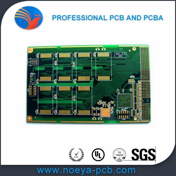

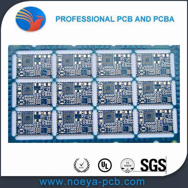
8 layer am fm radio pcb
Place of Origin: Guangdong, China (Mainland)
Brand Name: NOEYA
Model Number: Customized
Base Material: FR-4
Copper Thickness: 0.3OZ-4OZ
Board Thickness: 1.6mm
Min. Hole Size: 0.20mm
Min. Line Width: 0.1 0mm
Min. Line Spacing: 0.1mm4mil)
Surface Finishing: HASL Lead Free
Certificate: ISO/UL/TS16949/RoHS/TS16949
Solder mask: Green. Red. Blue. White. Black.Yellow
silkscreen: Green. Red. Blue. White. Black.Yellow
Describe
Packaging & Delivery:
Inner package: vacuum packing
Outer Package: Carton packing
Delivery: within 15 days after payment
Noeya pcb glance:
Noeya pcb capability:
| Capability | Standard | Advanced |
| Laminate | FR4, FR1, CEM-3, CEM-1, Aluminum, Rigid-Flex PCB, Teflon, High-TG, Rogers, Taconic | |
| Surface Finish |
HASL(vertical & Horizontal), Lead Free HASL ENIG,ENEPIG HASL+Gold Finger OSP / Entek Immersion Tin(ISN), Immersion Silver(IAG) Carborn Ink Hard Gold(Flash Gold), Soft Gold |
|
| Min. Thickness for inner layers | 0.020''-0.125'' | 0.003''(0.07mm) |
| Board layers | 1-24 Layers | 1-24 Layers |
| Board Thickness | 0.1mm-3mm | 0.2mm-7mm |
| Copper weight | 0.5 oz-6 oz | 0.5 oz-8 oz |
| Minimum Trace Width/Spacing | 0.003''/0.003'' | 0.003''/0.003'' |
| Solder Mask Color | Green, Blue, Black, Red, Yellow, White amd customized | |
| Drill deviation | 0.004'' |
±0.002''(0.05mm) |
| PTH Hole Tolerance | 0.004'' |
±0.002''(0.05mm) |
| NPTH hole Tolerance | 0.008'' |
±0.002''(0.005mm) |
| Min. hole size | 0.004'' | 0.008''(0.02mm) |
| E-test | Flying Probe Tester/Test-Jig/X-ray/ICT/AOI/FCT | |
| Controlled Tolerance |
±3% |
±3% |
| Silkscreen Color | White, Black, Yellow, Green, Red, Blue, and customized | |
| Min. Solder Mask clearance size | 0.008 | 0.003''(0.07mm) |
| Min. silkscreen clearance size | 0.010'' | 0.06''(0.15mm) |
| IPC Class | Class 2 | Class 3 |
| Blind Vias | YES | YES |
| Buried Vias | YES | YES |
| Aspect Ratio | 8/1 | 15/1 |
| Carbon Ink | YES | YES |
| Peelable Mask | YES | YES |
| Solder Sample | YES | YES |
| First Article | YES | YES |
| Certificate | UL / SGS / ROH / ISO / TS16949 / ISO14001:2004 | |
| Acceptable file format | GERBER File, PROTEL 99 / PADS / POWER PCB / AutoCAD / EAGLE | |
Details of PCB & PCBA
Technical requirement for pcb&pcb assembly:
---Professional Surface-mounting and Through-hole soldering Technology
---Various sizes like 1206,0805,0603 components SMT technology
---ICT(In Circuit Test),FCT(Functional Circuit Test) technology.
---PCB Assembly With UL,CE,FCC,Rohs Approval
---Nitrogen gas reflow soldering technology for SMT.
---High Standard SMT&Solder Assembly Line
---High density interconnected board placement technology capacity.
Quote requirement for pcb&pcb assembly:
---Gerber file and Bom list
---Clear pics of pcba or pcba sample for us
---Test method for PCBA
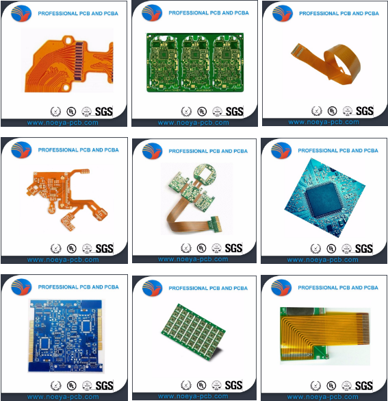
Related products
News
-
2019-02-14
Start Work of PCB and PCBA in 2019 , Good Luck !
Noeya Technology Ltd starts work of 2019 on 11th, Feb,2019.Wishing us the best of luck on r…
Read more -
 2019-01-14
Noeya's Annual Party
On 12nd, Jan 2019, Noeya hold an annual party, all people get together and have fun.
Read more -
 2018-12-21
2019 New Year and Holiday Notice
Noeya will have holidays from 29th,Jan 2019 to 10th, Feb,2019.We will back to work on 11st,…
Read more