

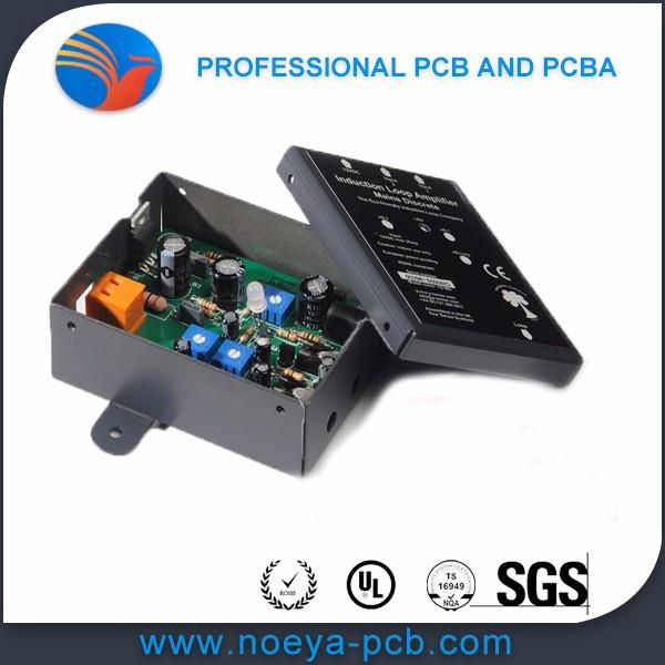

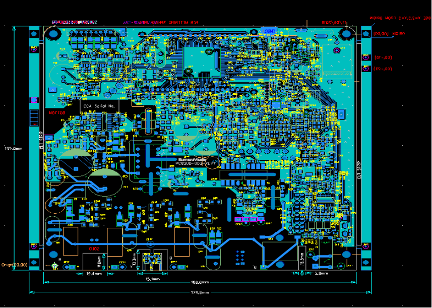
PCB Design
Describe
Capabilities & Services
*Schematic capture, bill of materials generation
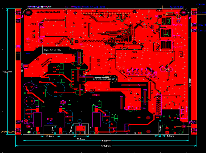
*Board artwork, SMT solder paste stencil artwork, CAM data generation
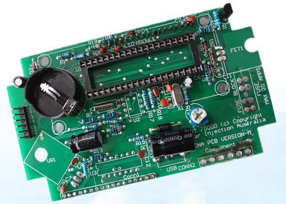
*Assembly drawings, fabrication drawings
*Multi-layer boards, split ground planes, differential pairs, high speed rules
*Routing per trace/space, keep-out, and clearance rules specified by customer
*Component resequencing based on physical layout, reverse annotation to schematic
*Schematic capture, bill of materials generation
*Board artwork, SMT solder paste stencil artwork, CAM data generation
*Assembly drawings, fabrication drawings
*Multi-layer boards, split ground planes, differential pairs, high speed rules
*Routing per trace/space, keep-out, and clearance rules specified by customer
*Component resequencing based on physical layout, reverse annotation to schematic
*DFT audit, test point placement, test probe clearance per customer rules, testability report
Related products
News
-
2019-02-14
Start Work of PCB and PCBA in 2019 , Good Luck !
Noeya Technology Ltd starts work of 2019 on 11th, Feb,2019.Wishing us the best of luck on r…
Read more -
 2019-01-14
Noeya's Annual Party
On 12nd, Jan 2019, Noeya hold an annual party, all people get together and have fun.
Read more -
 2018-12-21
2019 New Year and Holiday Notice
Noeya will have holidays from 29th,Jan 2019 to 10th, Feb,2019.We will back to work on 11st,…
Read more