


High Density Interconnect PCB
Describe
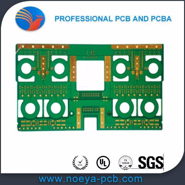
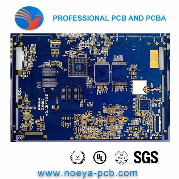
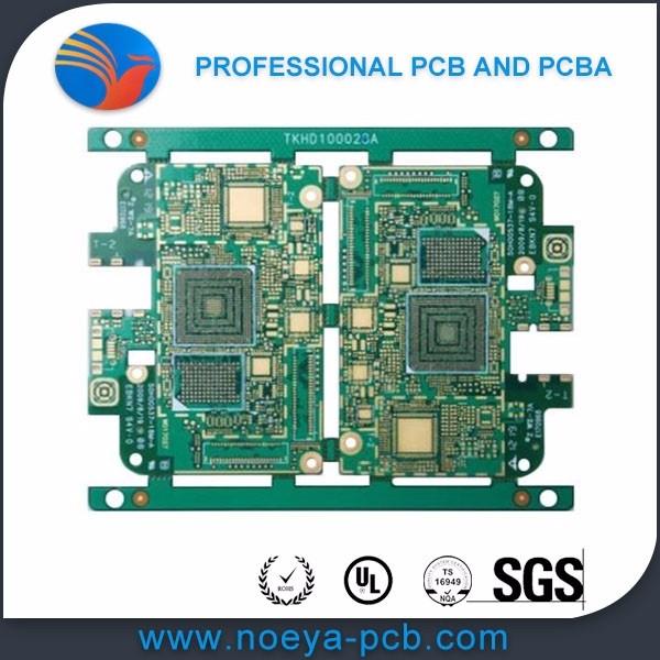
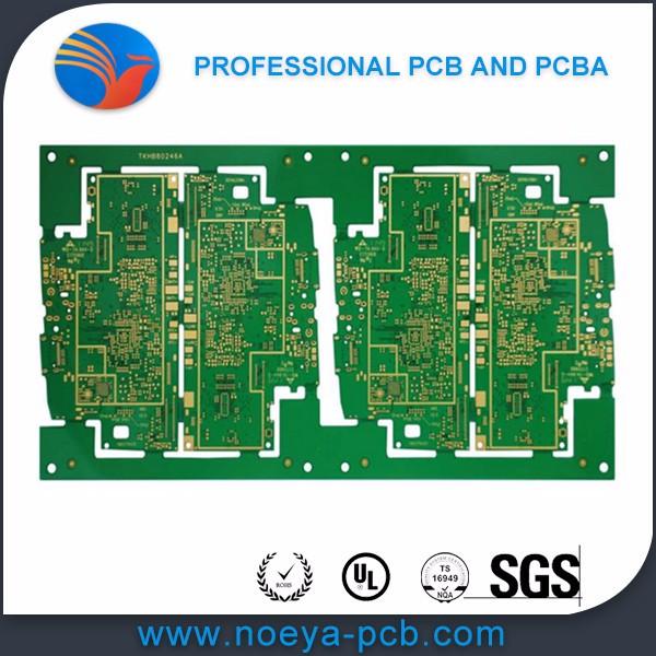
HDI (High Density Interconnect) PCB
Substrate or board with the Microvia of aperture below 6mil,
Hole pad below 0.25mm,
Connect pad density above 130 points / square inch,
Wiring density above 117 inches / square inch,
Line width / spacing below 3mil/3mil,
Mainly used in mobile phones, cameras, camcorders, laptops, network card, IC carrier board, military, medical and other different areas.
Specification:
1)Electronic Circuit PCB Board
2)Certificate: UL,SGS,RoHS,ISO/TS16949,ISO14001:2004
3)Base Material: High TG FR-4/FR-4/Lead Free Material(ROHS Compliant)/CEM-3/CEM-1/FR-1
4)Solder Mask: Green/Red/Yellow/Blue/Black/Customized
5)Surface Treatment: Lead Free HASL/HASL/ENIG/OSP/Customized
6)Packing Details: Vacuum+Dessicant
7)Competitive Price, High Quality
8)Fast Delivery: 5-10 working days
9)OEM Service
Our Capability

Purchase Tips:
1)Acceptable file format: GERBER file, PROTEL series, PADS series, POWER PCB series, AutoCAD series
2)Large PCB quantiy order, quotation will be based on SQM
3)Any requirement, feel free to contact us.
Related products
News
-
2019-02-14
Start Work of PCB and PCBA in 2019 , Good Luck !
Noeya Technology Ltd starts work of 2019 on 11th, Feb,2019.Wishing us the best of luck on r…
Read more -
 2019-01-14
Noeya's Annual Party
On 12nd, Jan 2019, Noeya hold an annual party, all people get together and have fun.
Read more -
 2018-12-21
2019 New Year and Holiday Notice
Noeya will have holidays from 29th,Jan 2019 to 10th, Feb,2019.We will back to work on 11st,…
Read more